Warning: working with high voltage like this is dangerous. This post is just for documenting my work and sharing knowledge. It is never intended as a tutorial.
Introduction
Recently, I had the need for an isolated 400V source for testing some circuits, and it needed to be ready in a weekend. I had a simple push-pull inverter based on IR2153 that I built back in high school for coilgun projects, but it wasn’t complete and didn’t have any forms of feedback. I also remember it drew a ton of current, something like 10+ amps at 12V, which would be bad for the MOSFETs and the transformer windings.
The plan would be to connect its output to a large (<1mF) capacitor and add a simple feedback mechanism to turn off the inverter when the desired output voltage is reached. I would also need to address its large input current so it can work with a 5A bench power supply.
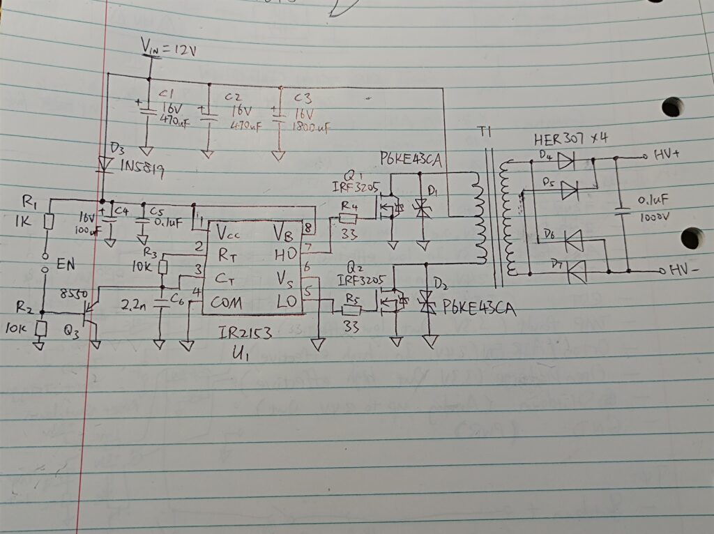
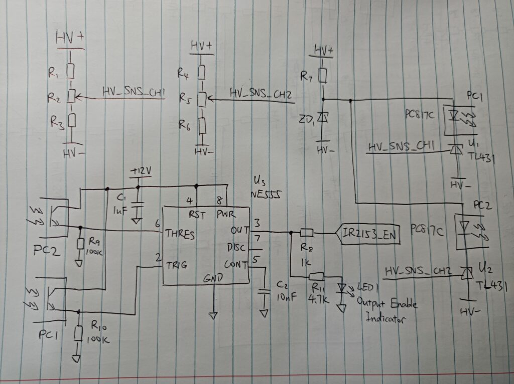
IR2153 is a simple oscillator with built-in MOSFET drivers and bootstrap circuits for driving a half-bridge up to 600V, with a fixed duty cycle of 50%. Due to its simplicity, it was popular among hobbyists for making simple tesla coils, induction heaters, coilgun high-voltage capacitor chargers, etc. I can’t remember where I found the schematic this was based on, but here is the schematic of what I built:
Back then, I also got myself some custom transformers made (it was only something like $40 for 20 transformers, including materials and labour) and one is used in this board. I’ve forgotten the turns ratio, so that’s also something I found out by measurements.
Transformer Measurements
The measurement plan was simple: apply a known voltage at the primary and measure the voltage at the secondary. In this test, I used a 30kHz square wave signal (same as the IR2153), with a 1K resistor between the signal generator and the transformer to limit the current.
Here is the scope capture:
With this setup, the primary voltage was about 0.17Vp-p and the secondary voltage was about 4.08Vp-p. That gives a turns ratio of 24. From memory, I probably specified the primary to have either 5+5 turns or 10+10 turns, and the secondary turns number was probably in the whole hundreds. Based on this information, the actual turns are probably 10+10 for the primary and 500 for the secondary. That would give a turns ratio of 25. When being used in a push-pull setup, the turns ratio would be 50.
Simple High Voltage Feedback and Control
Now, back to the main topic – voltage feedback. I didn’t need the output voltage to be very precise, so a simple hysteresis controller would serve the purpose. It works by turning off the IR2153 when the output voltage is too high and turning it back on when the voltage is too low. The time between on/off shouldn’t be too short, just to keep the IR2153 happy.
The circuit to sense whether the HV has reached a threshold was based on this:
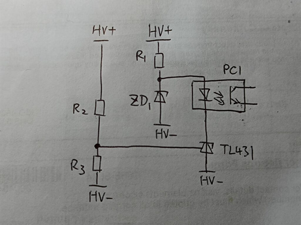
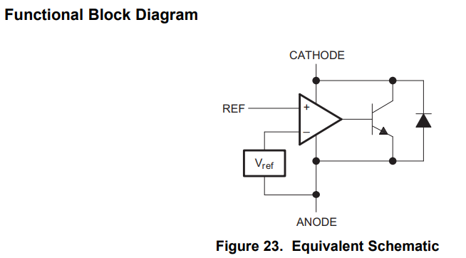
TL431 is a type of precision shunt regulator that I used as a comparator with a built-in 2.5V reference. From its datasheet, its equivalent schematic is as follows:
Combined with the circuit above, it’s clear that when the divided HV voltage goes above Vref of the TL431 (2.5V), the op-amp turns on and pulls its cathode to ground, activating the photocoupler. The Zener diode is there to limit the voltage across the TL431 when the transistor is off.
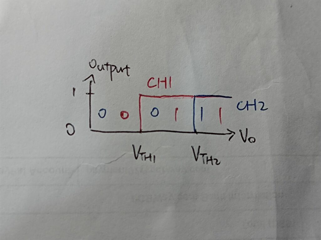
To achieve hysteresis, I would need two channels of the basic HV sensing. Let’s say they’re CH1 and CH2, and CH1 has a lower triggering voltage. Then their output logic is as follows:
If I invert CH1 to get this:
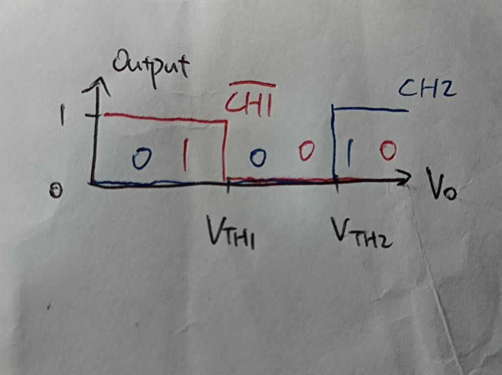
I can then feed the outputs into an SR latch to control the shutdown transistor controlling the IR2153, so that once the HV voltage goes above VTH2 the IR2153 will get turned off, and once the voltage falls below VTH1 the IR2153 will turn on again. When the voltage is between VTH1 and VTH2, the output remains at the previous state. The SR latch can be implemented using a simple 555 circuit. The overall circuit would look like this:
One drawback of this circuit is that the resistor for biasing the TL431 can’t be too large, as each of the TL431 requires a minimum cathode current of 0.4mA to function. With two of them, that means the bias resistor R1 would consume at least 0.32W of power at 400V. In reality, the current may not evenly distribute between the two devices, so a slightly higher current would be required to make sure both of them work. If I were to use an isolated power supply and comparators/op-amps to sense the voltage then this current can be much lower, but I didn’t have isolated supplies on hand.
Choosing Components
When selecting the sampling resistors, one would want to minimise the current to reduce power dissipation on those resistors. To select R1 ~ R3, consider the reference input current of TL431. From the datasheet:

I took the upper limit of 4uA and multiplied it by 10 to use as the voltage divider current (i.e., 40uA). For the low-side resistor, 2.5V divided by that 40uA gives 62.5KΩ, which I can achieve using 10KΩ for R3 and 100KΩ for R2. For R1, 400V divided by 40uA gives 10MΩ (to be exact, 400-2.5=397.5V should be used here, but the 2.5V is negligible really and the threshold is adjustable anyway). R4 ~ R6 would be the same as R1 ~ R3. R7 was chosen as 400V divided by, say 1.2mA, which approximates to 330KΩ.
The voltage of the Zener doesn’t really matter, as long as it’s larger than the minimum working voltage and smaller than the rated maximum cathode voltage of TL431, which are 2.5V and 36V, respectively. The photocoupler won’t get damaged at higher voltages, as its current is limited by R7. I used a 5.1V Zener here, but in a previous design with the same concept, a 12V Zener was used with no problems.
For the photocoupler, I was using what I had on hand, which is the PC817C. As the photocoupler is being as a switch, the CTR (Current Transfer Ratio) shouldn’t be a major consideration, and if the current gets too small, a Darlington transistor stage can be added to the low voltage side.
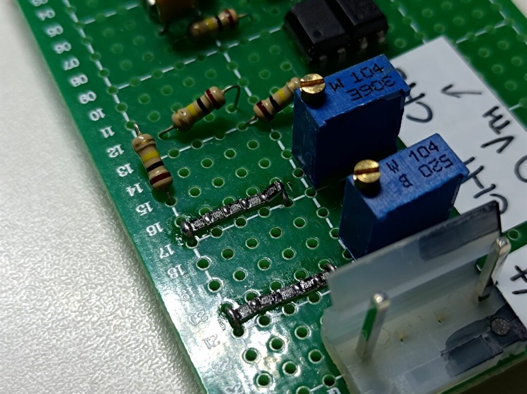
When building the circuit, an important consideration is how much voltage is across a resistor. Having multiple resistors can increase the creepage distance and help with distributing the generated heat. Based on what I have, for R1 and R4, I used 5x 2MΩ 0805 resistors, and for R7 I used 3x 100KΩ 1/4W through-hole resistors and a 33KΩ 0805 resistor.
Inverter Input Current Reduction
As mentioned above, the inverter drew a large current when charging up its output capacitor from 0V, as during startup, the output of the inverter is close to being shorted. There is a range of potential options for limiting the output current, but the quickest and simplest would be to add a capacitor in series with the transformer output, before the rectifier. The reactance of the capacitor would then limit the output current without introducing real power loss.
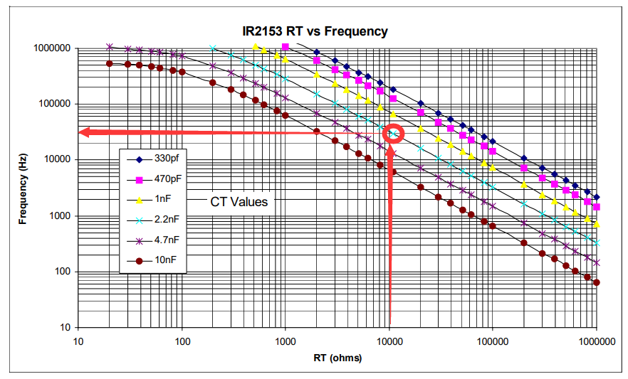
In my case, the IR2153 was configured with a 10KΩ/2.2nF combo for the oscillator. According to its datasheet, that would give a working frequency of about 30kHz:
For push-pull circuits, under ideal conditions, the output voltage would be Vin * D * 2 * (Ns/Np), where D is the driving duty cycle and Ns/Np is the transformer secondary/primary turns ratio. I used this as a starting point of how big the series capacitor should be.
At a 12V input, assuming the duty cycle is 50% (ignoring dead time), with a turns ratio of 50, the inverter output would be 600V. Making the input current less than 5A means a power limit of 60W, which translates to a maximum secondary current of 0.1A when the output is shorted. This would require a reactance of 6KΩ. At 30kHz, I would need a capacitance of ~0.9nF, so I put on a 1nF 2KV ceramic capacitor and tested it. Well, it turned out to be not sufficient, and after some iterative testing, I ended up putting two of 0.47nF in series. The short circuit input current then dropped to just over 5A at 12V.
It is worth noting that this capacitor needs to have a sufficient voltage rating, as during inverter startup the capacitors would have the full output voltage across them.
Building and Testing
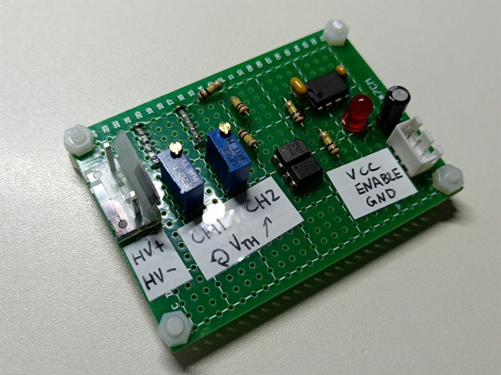
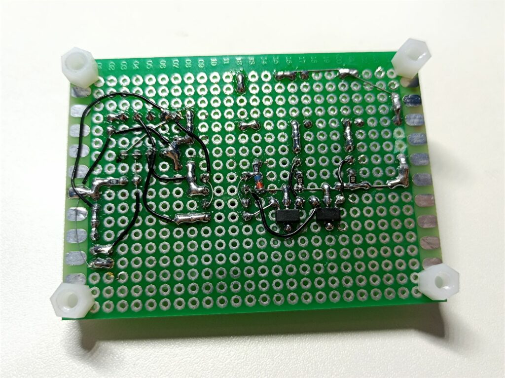
Building the controller was straightforward; For the 5x 2MΩ resistors, to maximise creepage distance, I soldered resistors one by one on the top side of the veroboard. If I were to solder on the bottom pads, the distance between the board pads would be shorter than the resistor pad spacing. For the HV input, I used a 3.96mm-pitched header with the middle two pins removed for isolation spacing. I also scraped the pads on the veroboard between the high voltage terminals to help increase the creepage distance.
When building the board I only had one PC817 left, so another one was salvaged from a dead power supply I had lying around.
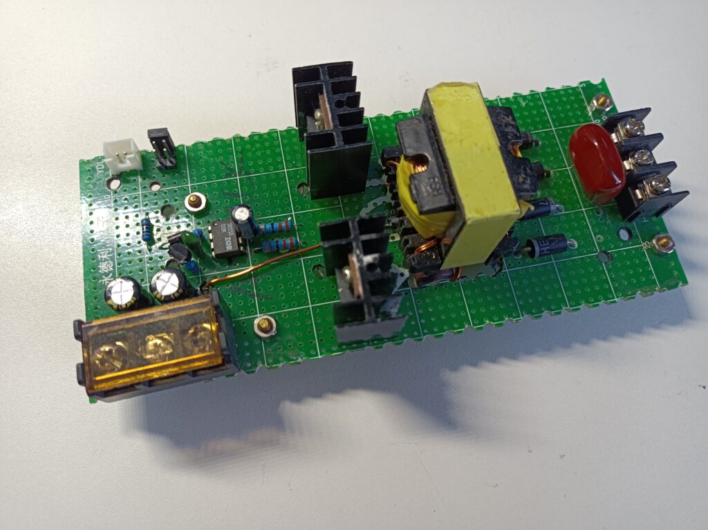
Here is the finished board:
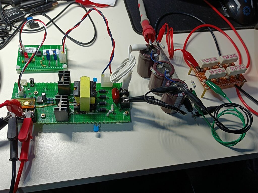
Here’s the testing setup. Just in case the voltage gets too high, I had three 450V 330uF capacitors in series as the load, each with a 300K 1W resistor soldered on, as the bleeding resistor. Other than this, I also added a resistor board which is made up of four 3.3K 5W resistors in series, for discharging the capacitors quickly.
To set the POT positions, these were the steps I took:
- Separate the IR2153 supply rail and the push-pull power rail (they were connected together).
- Set the CH1 threshold voltage all the way down. In my build, turning clockwise will increase the threshold, so in this step, I turned the CH1 POT counter-clockwise all the way. This sets the turn-on threshold.
- Set the CH2 threshold voltage all the way up. This sets the turn-off threshold.
- Supply 12V to the IR2153.
- Supply the main power rail with something like 5V (the UVLO threshold of IR2153 is ~10V, hence the separation in the first step) to get a lower open-loop output voltage.
- Slowly increase the main power rail voltage until the desired output turn-off voltage is reached.
- Slowly decrease the CH2 threshold until the controller starts to turn off the inverter
- Slowly increase the CH1 threshold until the turn-on voltage reaches the desired value.
An Alternative Design
Another idea that I considered during the design was to use a transistor current source circuit and use the photocoupler to transmit the voltage information in analog. The circuit normally works as a constant current sink, but the voltage across the bias diodes won’t truly stay constant as the voltage changes. As a result, that will make the photocoupler current vary slightly with the applied voltage. As it’s a current sink, it can work across a wider range of voltage compared to my current design, where the lowest output voltage would be limited by the minimum TL431 cathode current. Again, my options were limited by parts availability, as I didn’t have any sufficiently rated high-voltage transistors for this design.
Here’s a basic LTSpice simulation showing this idea in action. The blue trace represents the inverter output voltage changing between 50V and 450V, and the green trace is the current through the output resistor.
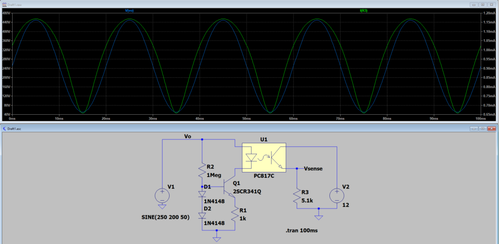
With the components in this simulation, the output current ranges between 0.65mA and 1.17mA, which will cause a fairly large voltage variation across a 5.1K resistor for feeding into a Schmitt trigger. The highest total current consumption on the HV side at 450V is also less than 1mA, which is better than my current design of 1.3mA at 400V. Another potential is that I can read the photocoupler output using a microcontroller, compensate for the nonlinearity, and provide a way to digitally set the inverter output voltage. That would be quite nice as I’m still interested in coilguns and hope to get back into it one day 🙂